


SOLID STATE
SOLIDS
Solid substances are characterised by definite shape, volume, rigidity, high density, low compressibility, mechanical strength, slow diffusion and hard nature. The constituent particles (atoms, molecules or ions) are closely packed and held together by strong forces.
CRYSTALLINE SOLIDS
The constituent particles are arranged in definite geometrical pattern i.e. they have lattice structure.
AMORPHOUS SOLIDS
They have random arrangement of the constituent particles (amorphous - means without any form).
DIFFERENCES BETWEEN CRYSTALLINE AND AMORPHOUS SOLIDS
Crystalline
|
Amorphous
|
Have lattice structure
|
Do not have lattice structure
|
Have sharp melting point
|
No sharp melting point
|
They are anisotropic i.e. their physical properties are different along different directions
|
They are isotropic i.e. their physical properties are the same along all directions
|
They are symmetrical
|
They are non symmetrical.
They are supercooled liquids |
Show clean cleavage
|
No clean cleavage
|
Examples: Diamond, NaCl, etc.
|
Examples: Glass, Rubber, Plastic
|
CRYSTAL LATTICE
The three dimensional orderly arrangement of constituent particles of a crystalline solid is known as Crystal lattice.
UNIT CELL
The smallest geometrical portion of the crystal lattice which can be used as repetitive unit to build up the whole crystal is called unit cell.
TYPES OF UNIT CELL
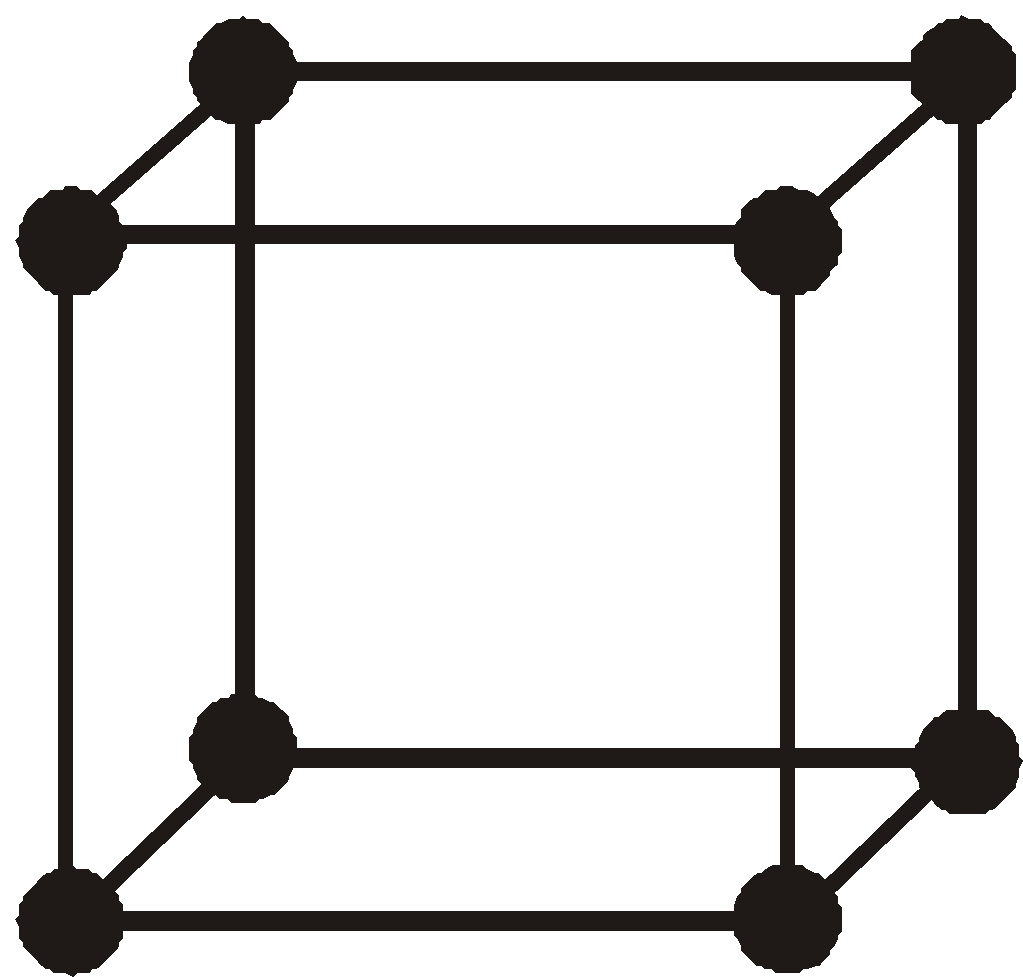
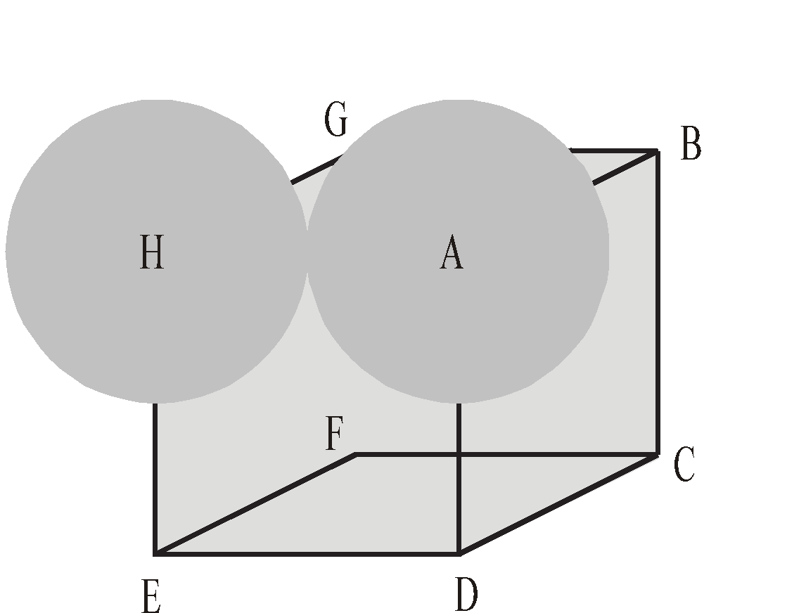
SIMPLE OR PRIMITIVE : Unit cell in which the particles are present at the corners only
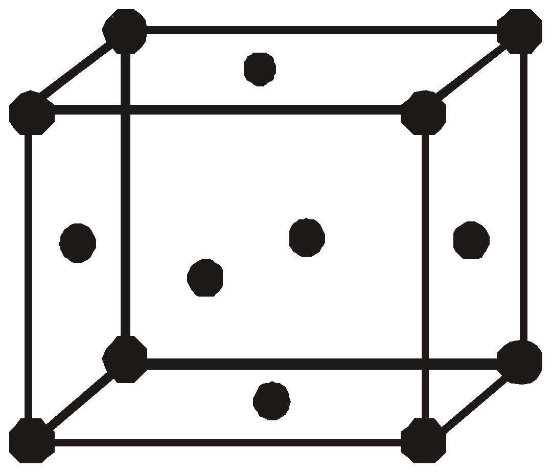
FACE CENTRED : In which the particles are present at the corners & at the centre of each of six faces.
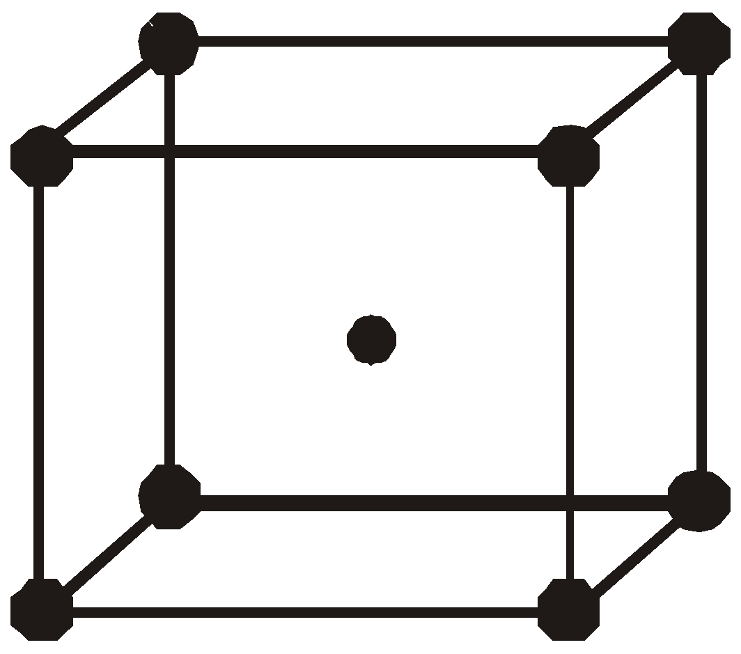
BODY CENTRED : In which the particles are present at the corners and in the centre.
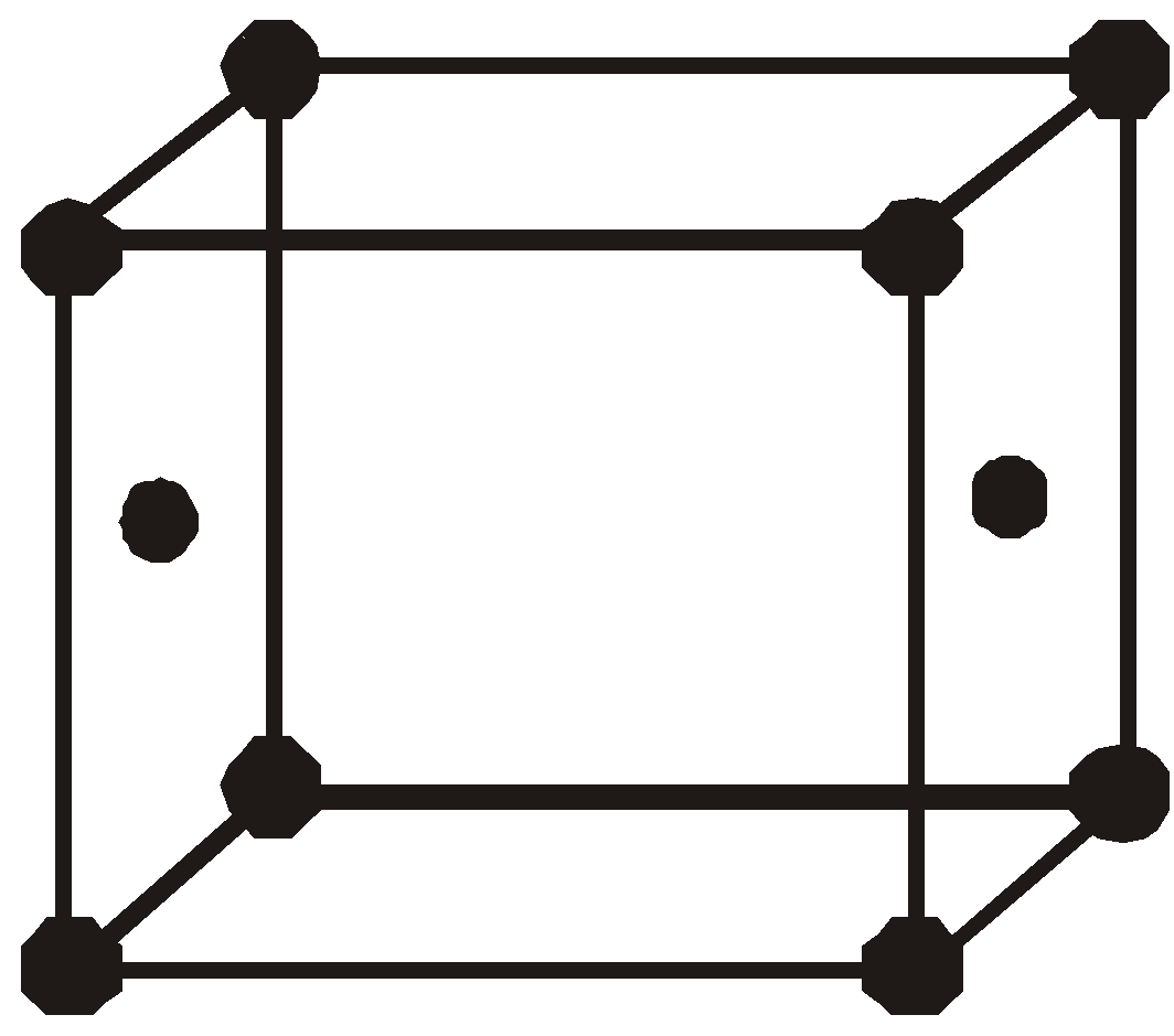
END FACE CENTRED : In which the particles are present at the corners and at the centre of two opposite faces.
PACKING FRACTION
It is defined as the ratio of the volume of the unit cell that is occupied by the spheres to the volume of the unit cell.
PRIMITIVE CUBIC UNIT CELL : Number of atoms per unit cell = 1
Atoms touch each other along edges.
Hence r = 
(r = radius of atom and a = edge length)
(r = radius of atom and a = edge length)
Therefore P.F. =
FACE CENTRED CUBIC UNIT CELL : Number of atoms per unit cell = 4
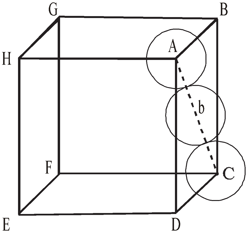
Atoms touch each other along the face diagonal.
Hence r =  (length of face diagonal =
  )
)
Therefore P.F. = 
BODY CENTRED CUBIC UNIT CELL : Number of atoms per unit cell = 2.
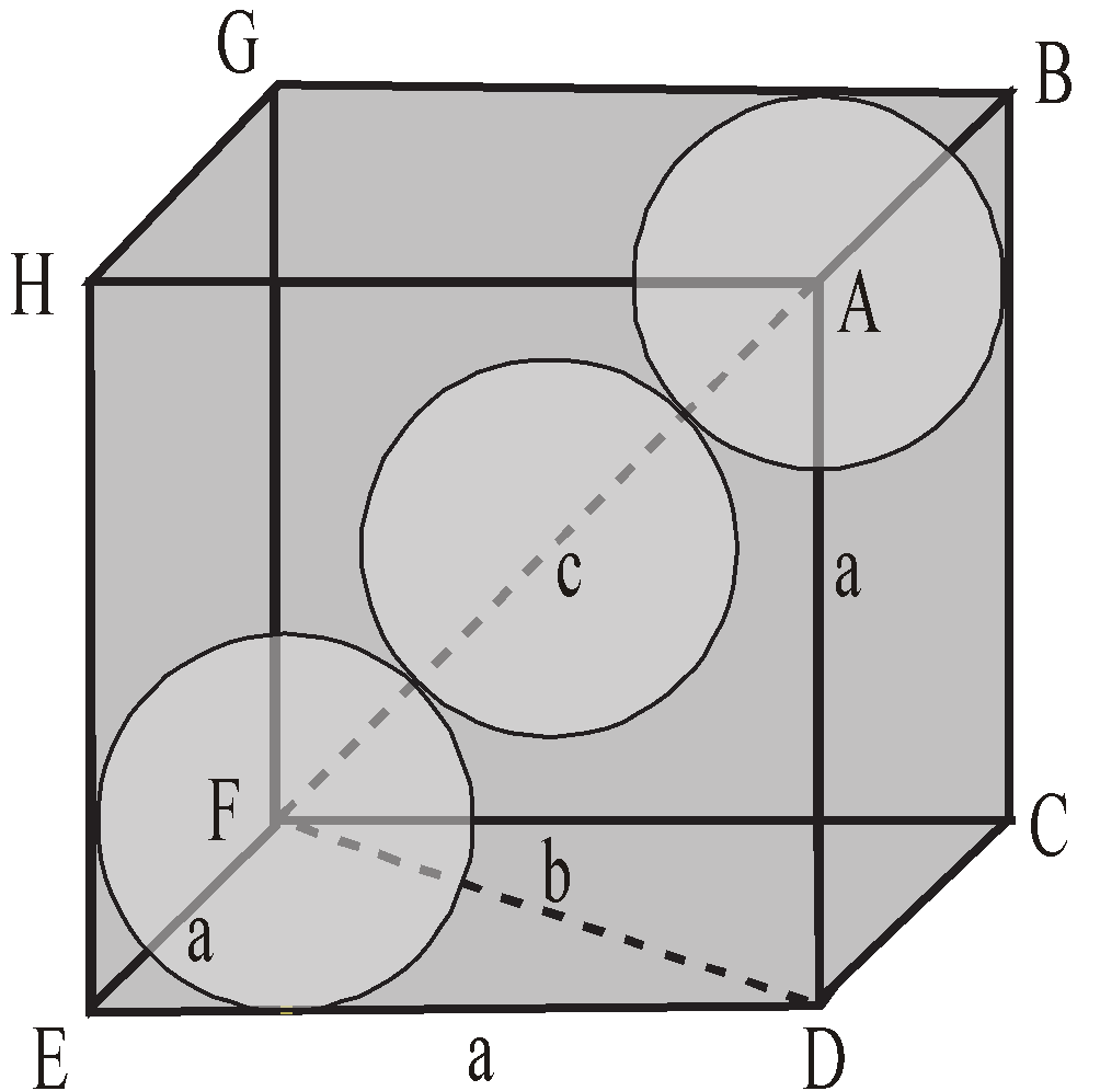
Atoms touch each other along the body diagonal.
Hence r =  (length of body diagonal =
  )
)
Therefore P.F. = 
HEXAGONAL PRIMITIVE UNIT CELL
Each corner atom is being shared by 6 other unit cells therefore their contribution to one unit cell would be .
.
Total number of atoms per unit cell 
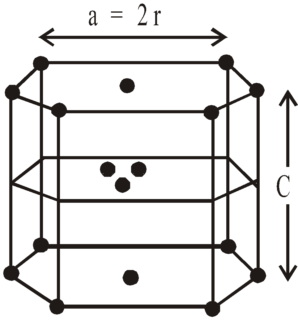
Height of unit cell C = 
Length of unit cell a = 2r
Area of base = area of six equilateral triangles
= 
Volume of unit cell = 
PF = 
SIZE AND SHAPE OF CRYSTALS
The slower the rate of formation of crystal, the bigger is the size of crystal and vice versa.
INTERFACIAL ANGLES
The angle between any two faces is called an interfacial angle. Interfacial angle remains the same in the same substance although the size of faces or even shape of crystal may vary.
LAW OF RATIONALITY OF INDICES OR INTERCEPTS
The ratio between intercepts on crystallographic axes for the different faces of a crystal can always be expressed by rational numbers.
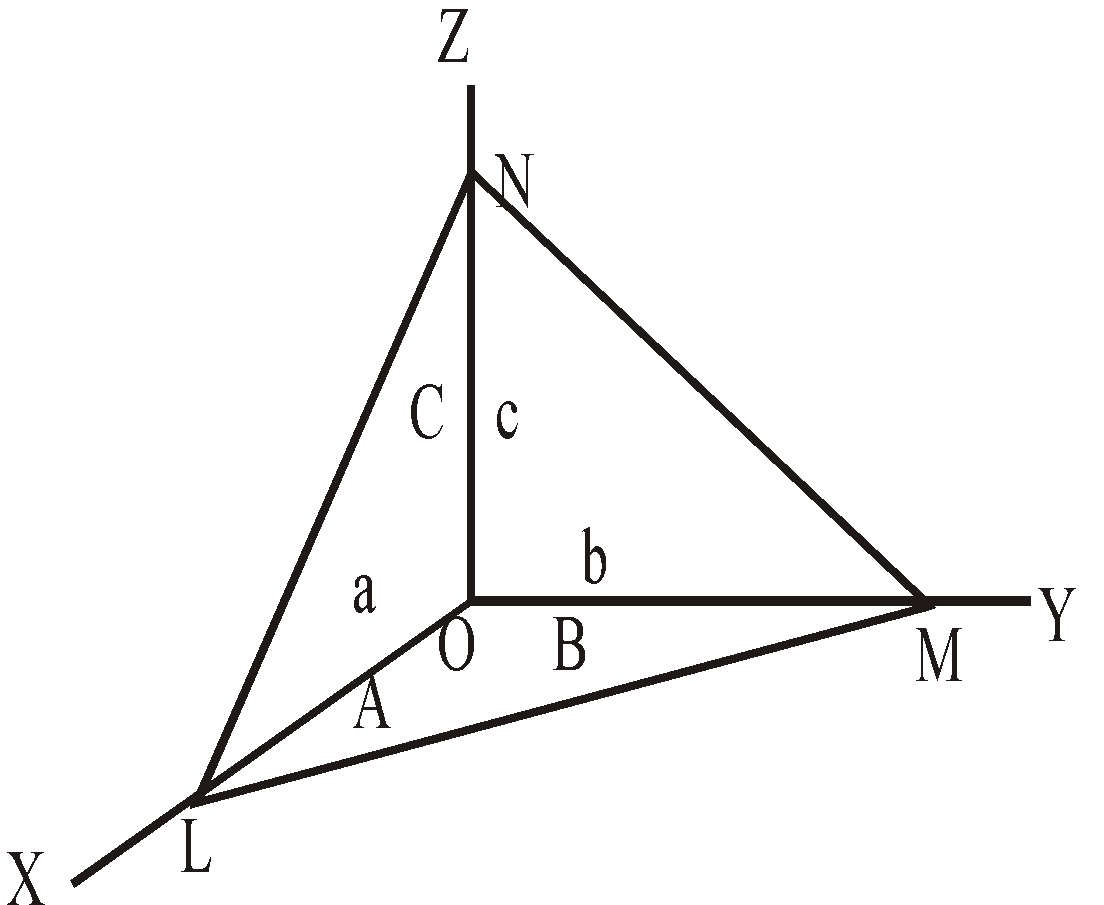
The plane LMN has intercepts OL, OM and ON along X, Y and Z axes of lengths 2a, 4b and 3c respectively. When OA = a, OB = b and OC = c are taken as unit distances, the intercepts are in the ratio 2a : 4b : 3c and coefficients of a, b and c are known as WEISS INDICES.
Weiss indices may have any values integers, fractional or infinity.
MILLER INDICES
Reciprocals of Weiss indices and multiplying throughout by smallest number to make integers are known Miller indices and represented by h, k and l and the plane as (hkl). For example, in (112) plane h = 1, k = 1 and l = 2.
The distance between the parallel planes in a crystal is designated as dhkl. For different cubic lattices the interplanar distances are given by
where a = length of cube side and h, k and l are Miller indices.
CRYSTALLOGRAPHIC AXES
The three mutually perpendicular lines meeting at a common point are called crystallographic axes. The angles between the axes opposite to the intercepts a, b, c on crystallographic axes are represented by  ,
,  and
and  . If axes coincide with or are parallel to the edges of crystal faces, then , ,
  will be the same as interfacial angles.
LAW OF RATIONAL INDICES
Consider a cubic unit cell, crystallographic axes, intercepts, faces represented as follows:
X, Y and Z are crystallographic axes meeting at O.
Let LMN be a unit plane having intercepts a, b and c on X, Y and Z axis.
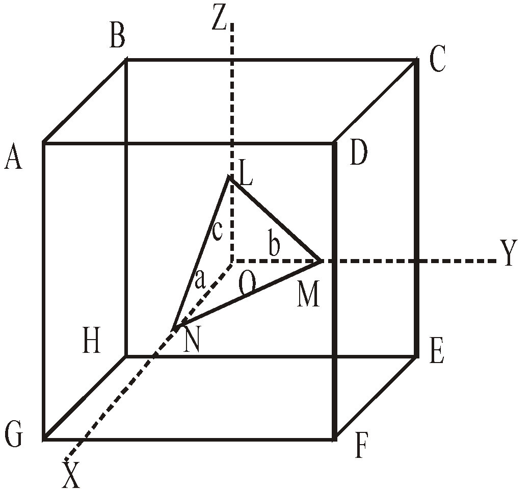
Intercepts of axis X :
- On face ADFG will be multiple of a
- On face BCEH will be multiple of 'a' with negative sign since it is in opposite direction (negative value is represented by putting a bar over it)
- On the faces ABHG and DCEF will be ∞ since X-axis can never cut these faces.
Intercepts of axis Y :
- On face DCEF will be multiple of b
- On face ABHG will be multiple of b with negative sign since in opposite direction
- On faces ABCD and EFGH will be ∞ since Y-axis can never cut these faces
Intercepts of axis Z :
- On face ABCD will be multiple of C.
- On face EFGH will be multiple of C with negative sign since in opposite direction.
- On faces ABHG and DCEF will be ∞ since Z-axis can never cut these faces.
CRYSTALLOGRAPHY AND X-RAY DIFFRACTION
(BRAGG'S EQUATION)
When X-rays strike the parallel planes of the crystal at an angle  , they are reflected from different planes. The resulting reflected beam will be strong if all reflected rays are in phase. Now as
Phase difference = 
If path difference is an integral multiple (say n) of wavelength, then phase difference becomes an integral multiple of 2p or 360° and hence the reflected rays will be in same phase
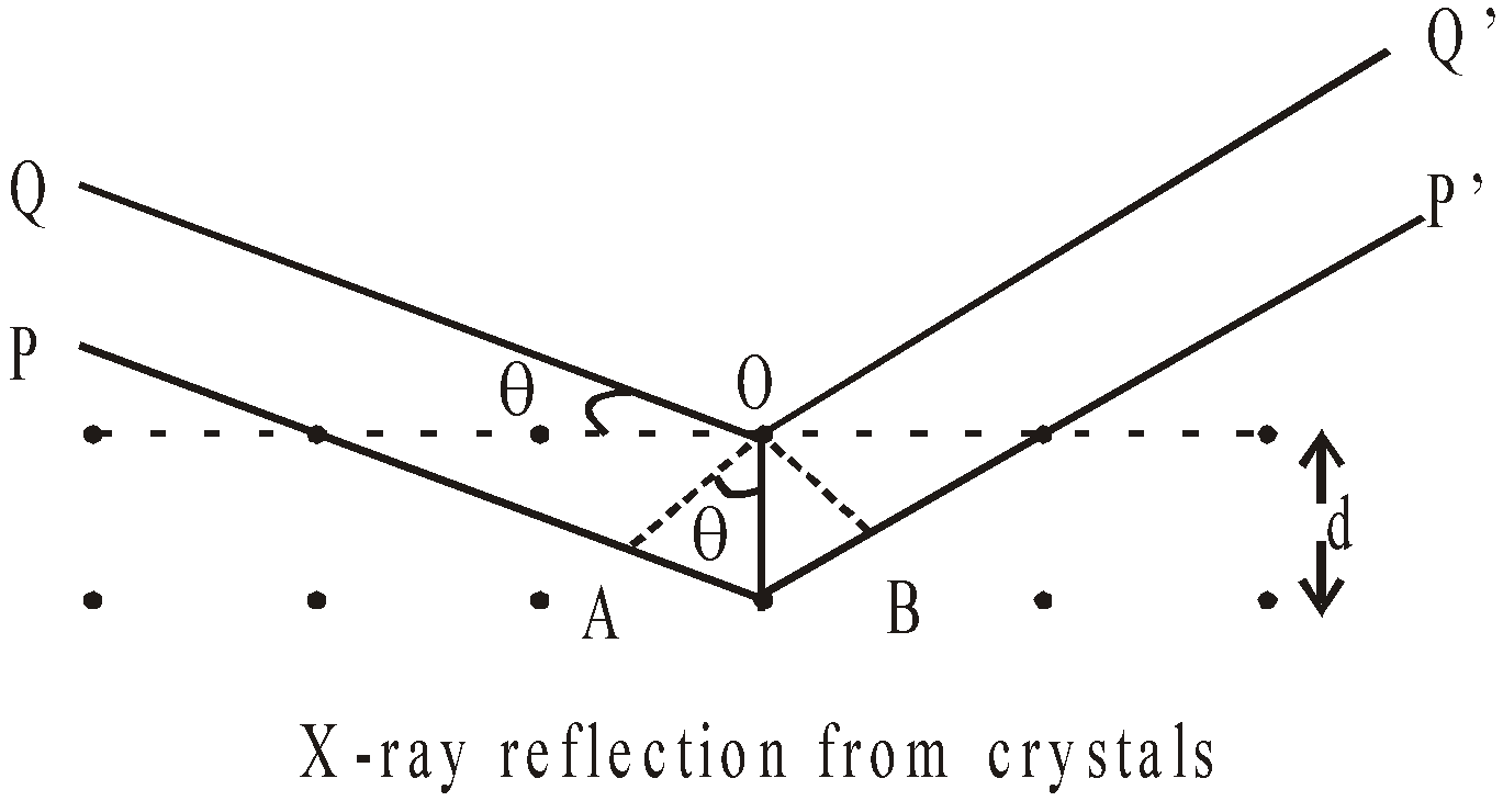
Now from figure the path difference between waves reflected from upper planes = AO + OB
From simple trigonometry, if d is the distance between successive layers then sin = 
OA = d sin
Similarly OB = d sin
Thus net path difference = OA + OB = 2d sin
Now for maximum reflection condition (defined above)
path difference = n × wavelength
2d . sin = n
This is Bragg's equation.
SYMMETRY IN CRYSTAL SYSTEMS
- Plane of symmetry : Which divides a crystal in two parts in such a way that one part is the mirror image of the other.
- Axis of symmetry : It is a line about which the crystal may be rotated such that it presents the same appearance more than once during complete revolution.
- Centre of symmetry : It is a point such that any line drawn through it intersects the surface of the crystal at equal distances in both directions.
ELEMENTS OF SYMMETRY
Total number of planes, axes and centre of symmetries present in a crystal are termed as elements of symmetry. A cubic crystal of NaCl possesses 23 elements of symmetry.
- Planes of symmetry = 3 + 6 = 9
- Axes of symmetry = 3 + 4 + 6 = 13
- Centre of symmetry = 1
- Total number of symmetry elements = 23
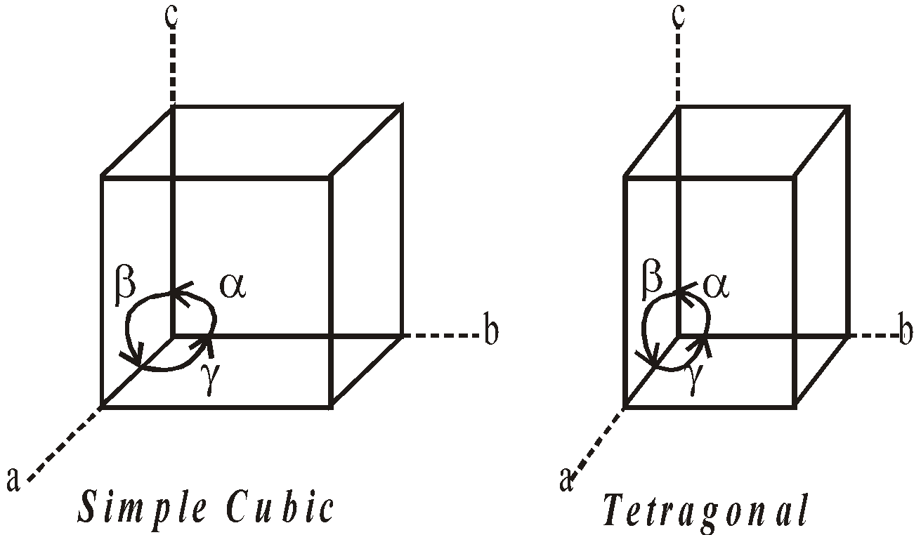
SEVEN CRYSTAL SYSTEMS
There are about 230 crystal forms, which have been grouped into 14 types of space lattices called BRAVAIS LATTICES on the basis of their symmetry and 7 different crystal systems on the basis of interfacial angles and axes.
Crystal System
|
Intercepts/Axes
|
Angles
|
Bravais
Lattices
| |
1.
|
Cubic
|
a = b = c
|
3 Primitive, Face Centred, Body centred
| |
2.
|
Tetragonal
|
2 Primitive, Body centred
| ||
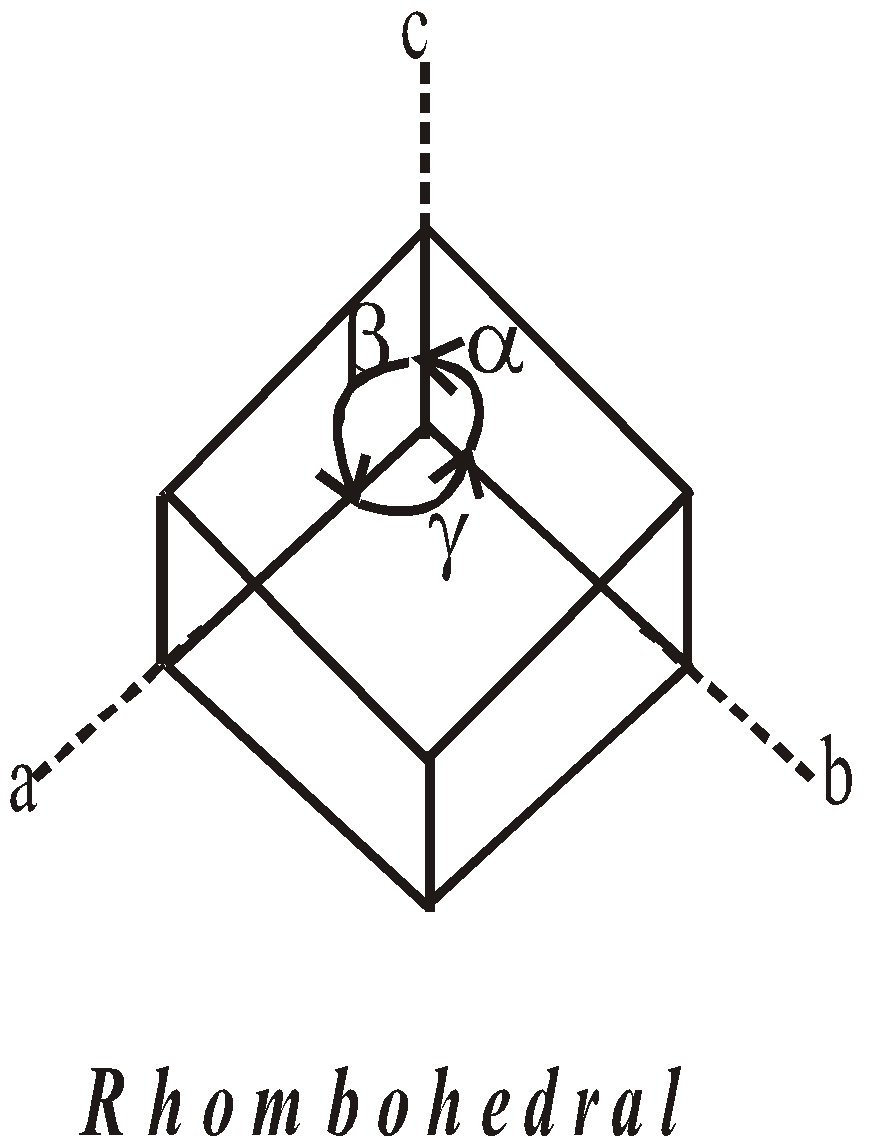
3.
|
Rhombohedral
|
a = b = c
|
1 Primitive
| |
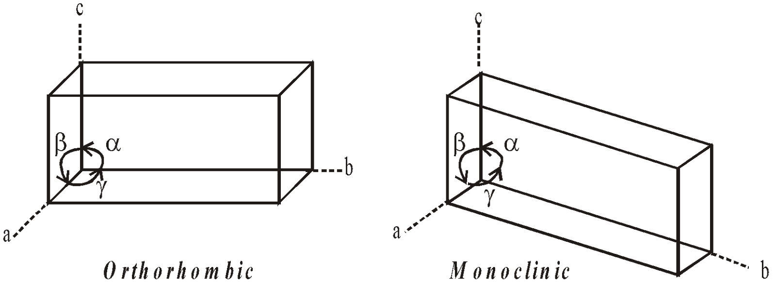
4.
|
Ortho Rhombic
|
4 Primitive, Face centred, Body centred, End centred
| ||
5.
|
Monoclinic
|
2 Primitive, End Centred
| ||
6.
|
Triclinic
|
1 Primitive
| ||
7.
|
Hexagonal
|
1 Primitive
|
TYPES OF UNIT CELLS OCCURRING IN CRYSTALS
Bravais showed from geometrical considerations that there are only 7 shapes in which unit cells can exist. These are:-
- Cubic
- Orthorhombic
- Rhombohedral
- Hexagonal
- Tetragonal
- Monoclinic
- Triclinic
On the basis of presence of particles there are 4 types of unit cells
- Primitive or simple
- Face centred
- Body centred
- End centred
He also showed that out of possible 28 unit cells (Seven shapes × four types in each shape = 28) only 14 actually exists. These are called BRAVAIS LATTICES.
CO-ORDINATION NUMBER
It is defined as the number of particles immediately adjacent to each particle in the crystal lattice.
- In simple cubic lattice C.N. is 6
- In body centred lattice C.N. is 8 and
- In face centred cubic lattice C.N. is 12.
High pressure increases C.N. and high temperature decreases the C.N.
PACKING OF CONSTITUENT PARTICLES IN CRYSTALS
Generally the particles of larger size do the packing and particles of smaller size occupy interstitial places
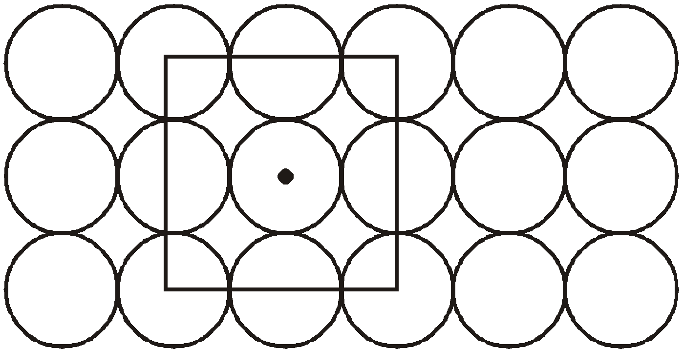
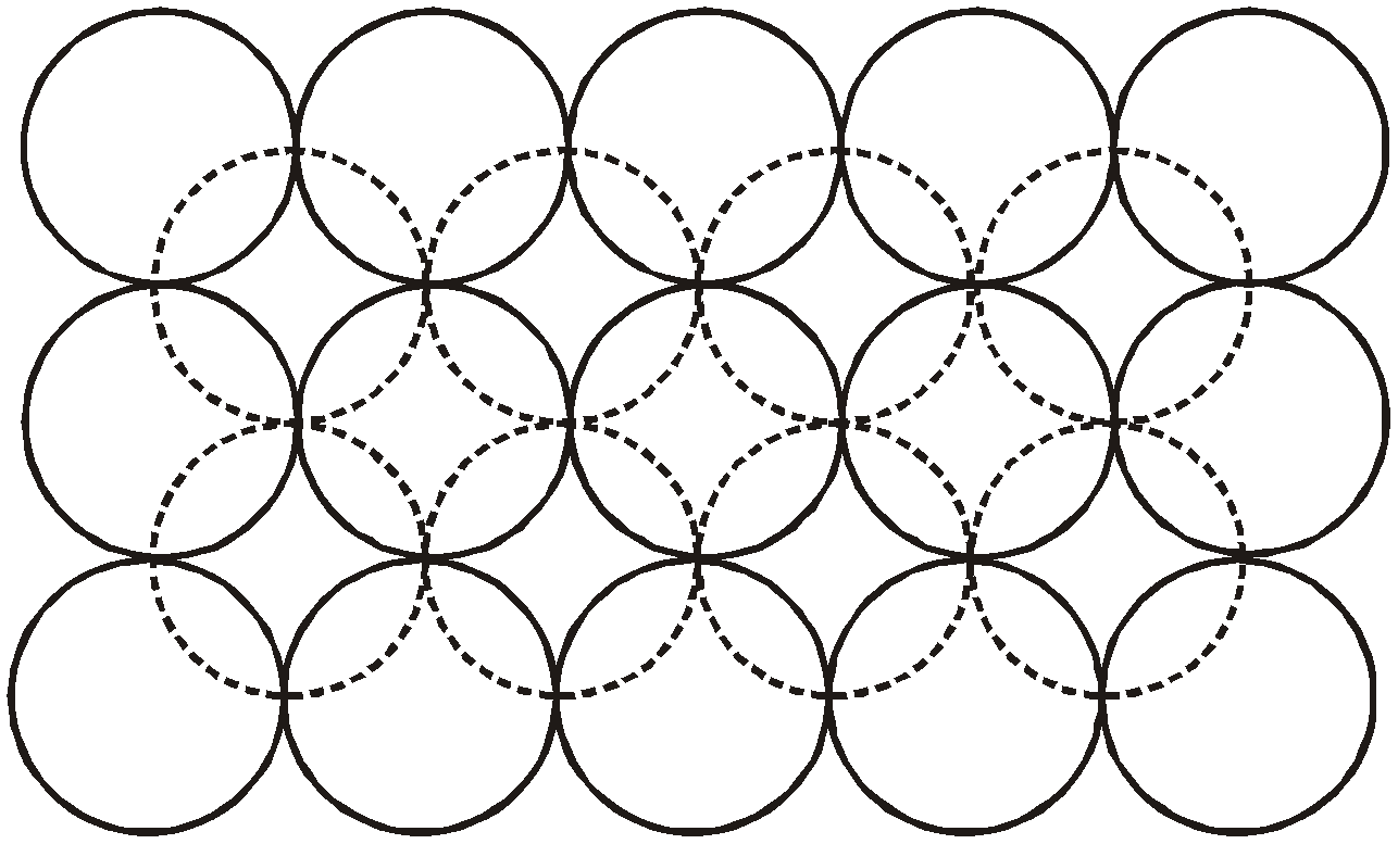
CLOSE PACKING IN TWO DIMENSIONS
It is of two types-
Square close packing
Space occupied by spheres is 52.4%
Space occupied by spheres is 52.4%
Hexagonal close packing
Space occupied by spheres is 60.4%.
Hence it is more efficient.
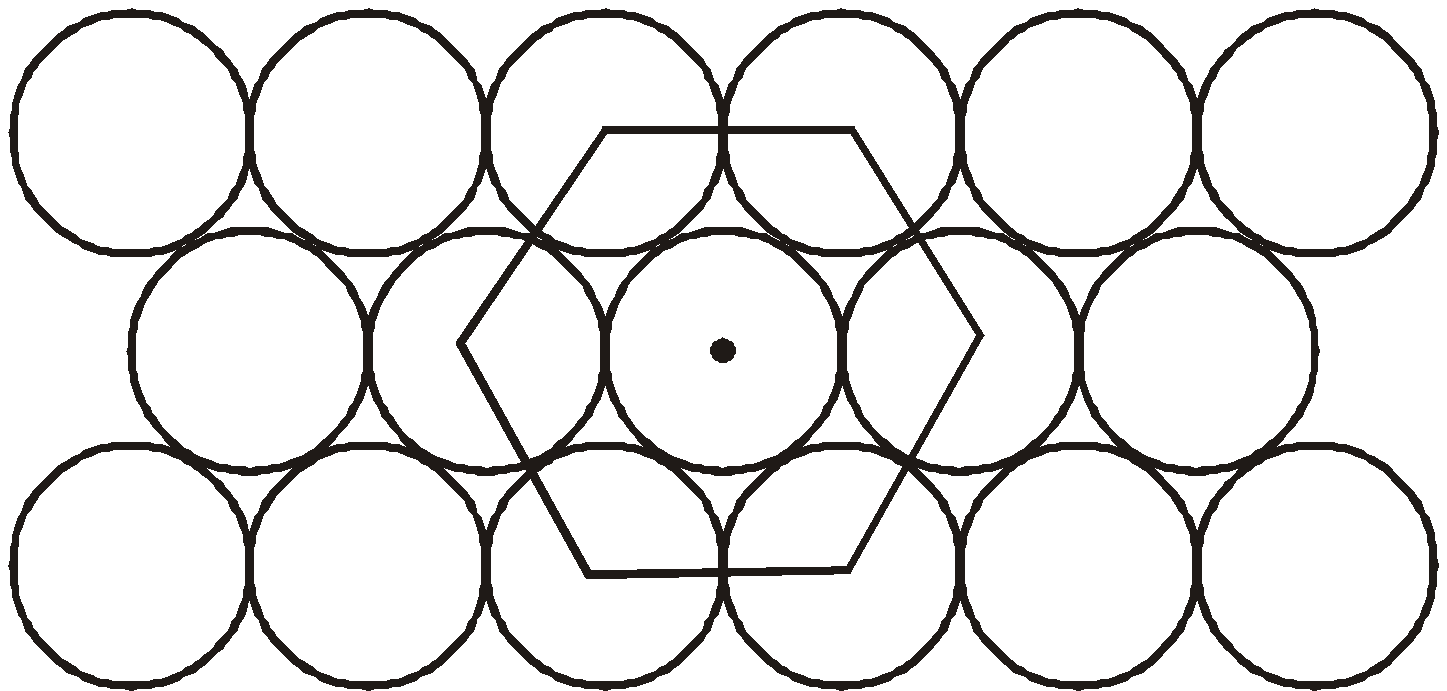
CLOSE PACKING IN THREE DIMENSIONS
Following the hexagonal close packing here, we have two layers.
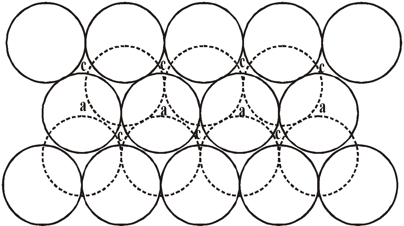
For third layer there are two types of voids, marked a tetrahedral voids and marked c octahedral voids. If spheres are placed over a, first layer is repeated and we have AB- AB arrangement. This is known as hexagonal close packing (hcp). If spheres for third layer are placed over c, a different layer is formed and we have ABC-ABC arrangement. This is known as cubic close packing (ccp).
Both hcp and ccp are equally efficient and space occupied by spheres is 74.0%. The cubic close packing has face centered cubic (fcc) unit cell.
Following the square close packing in three dimensions, we have AB, AB arrangement of spheres.
The resulting structure in this arrangement is referred to as body centred cube (bcc). In this arrangement only 68% of the available space is occupied by spheres and occur in many solids.
INTERSTITIAL VOIDS
The space left after hcp and ccp (74.0% in each case) is known as interstitial voids. They are of two types:
TETRAHEDRAL VOIDS : The vacant space touching four spheres is called tetrahedral void. The radius ratio is
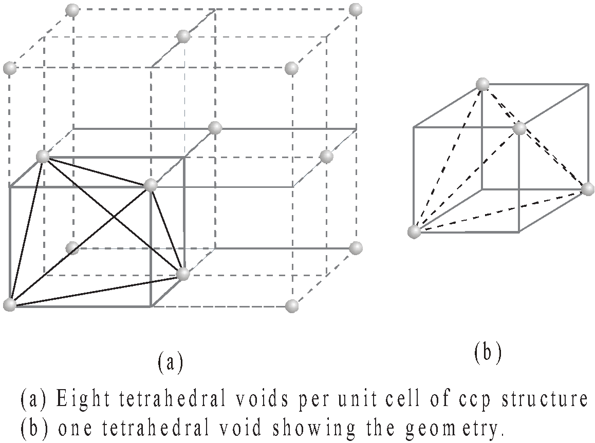
The number of tetrahedral voids is twice the number of spheres (atoms).
OCTAHEDRAL VOIDS : The vacant space touching six spheres is called octahedral void.
The radius ratio is 
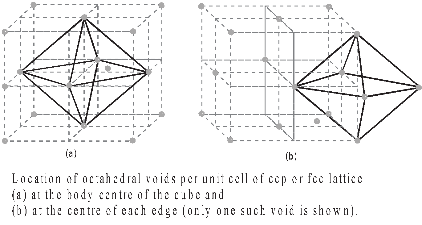
The number of octahedral voids is equal to the number of spheres (atoms).
LIMITING RADIUS RATIO
Cations tend to get surrounded by the largest number of anions.
Therefore, the larger the ratio, the larger is the coordination number.
Limiting radius ratio(r+/r–)
|
Shape
|
Coordination number
|
Example
|
0.155 – 0.225
|
Planar triangle
|
3
|
B2O3
|
0.225 – 0.414
|
Tetrahedral
|
4
|
ZnS
|
0.414 – 0.732
|
Square planar
|
4
| |
0.414 – 0.732
|
Octahedral
|
6
|
NaCl
|
0.732 – 1.000
|
Body Centred Cubic
|
8
|
CsCl
|
PRESENCE OF CATIONS AND ANIONS IN UNIT CELL
Crystal Structure
|
Anion
|
Cation
|
NaCl
|
8 at corners 6 at faces
|
12 at edges, 1 in body
|
ZnS
|
8 at corners 6 at faces
|
4 in body
|
CsCl
|
8 at corners
|
1 in body
|
CaF2
|
8 in body
|
8 at corners, 6 at faces
|
LATTICES OF SOME ELEMENTS
- Cubic close packed lattice : Cu, Ag, Au, Fe, Ni, Al
- Hexagonal close packed lattice : Zn, Cd, Hg, Be, Mg, Ti
In both the above structures each atom is surrounded by twelve nearest touching neighbours hence coordination number is 12.
- Body centred cubic lattice : Li, Na, K, Rb, Cs, W, Cr
This packing is not so tight as the first two are, each atom is surrounded by eight nearest touching neighbours, hence coordination number is 8.
RELATION BETWEEN EDGE OF UNIT CELL AND RADIUS OF CATION AND ANION IN FCC STRUCTURE
In NaCl structure, distance between cation and anion 
BODY DIAGONAL
In CsCl ions touch along body diagonal :
FACE DIAGONAL
If there is cube of edge length a then face diagonal is , Body diagonal is
  .
.
COORDINATION NUMBER OF AN ATOM IN
- Primitive cubic unit cell = 6
- Body centred cubic unit cell = 8
- Face centred cubic unit cell = 12
NORMAL SPINEL STRUCTURE
The mineral MgAl2O3 is known as spinel. The oxide ions are arranged in ccp, Mg++ ions occupy tetrahedral voids and Al+++ ions occupy the octahedral voids. Ferrite ZnFe2O4 has spinel structure. Being magnetic these are used in telephones and memory loops in computers.
INVERSE SPINEL STRUCTURE
Divalent ions occupy octahedral voids and trivalent ions are equally distributed in tetrahedral and octahedral voids. e.g. Fe3O4 or FeO. Fe2O3.
DENSITY OF UNIT CELL
where Z = Number of formula units present in unit cell. It is also known as rank or unit cell content.
M = Molecular weight, NA = Avogadro number
a = edge length of unit cell in pm
IMPERFECTIONS IN SOLIDS
They are of two types:-
ELECTRONIC IMPERFECTIONS
In Crystals of pure Silicon or Germanium some electrons are released from covalent bonds at temperatures above 0K which are now free to move in the crystal. The electron deficient bonds produced are known as holes.
Electrons (e) and holes (h) in solids are considered to be electronic imperfections. Concentrations of electrons (e) and holes (h) is represented by n and p.
ATOMIC IMPERFECTIONS
Further they may be divided as
- Point imperfections : The periodic arrangement of constituent particles is disturbed.
- Lattice imperfections : The deviations from periodic arrangement extend over microscopic regions of the crystal.
- Line defects / dislocations : The lattice imperfections extend along lines.
- Plane defects : The lattice imperfections extend along surfaces of crystals.
STOICHIOMETRIC POINT DEFECTS
SCHOTTKY DEFECT
It is due to missing of ion pairs (one cation and one anion) from their lattice sites. It maintains the electrical neutrality. Density of crystal decrease. It is more common in compounds with high coordination number and when size of positive and negative ions is almost equal. Example NaCl, KCl, CsCl and KBr etc.
FRENKEL DEFECT
It is due to dislocation of ion from its usual site to interstitial position. Density remains the same. It is common in compounds having low coordination number and large difference in size of +ve and –ve ions. Examples ZnS, AgCl, AgBr and AgI.
AgBr shows both of the above defects.
NON STOICHIOMETRIC POINT DEFECTS
METAL EXCESS (DUE TO ANION VACANCY)
It is due to absence of anion from lattice site leaving a hole which is occupied by electron to maintain electrical neutrality
A+ B– A+ B–
B– A+ e– A+
F-Centres - Holes occupied by electrons are called F-Centres (Colour centres). The greater the number of F-centres the greater is the intensity of colour of solid and solids are paramagnetic in nature. Due to F-centres
NaCl is yellow
KCl is violet
LiCl is pink.
Crystals showing schottky defect also show this defect.
METAL EXCESS DUE TO INTERSTITIAL CATIONS
It is due to extra positive ion and an electron occupying an interstitial position
A+ B– A+ B–
A+ e–
B– A+ B– A+
Crystals exhibiting Frenkel defect show this defect e.g.:- ZnO.
METAL DEFICIENCY DUE TO CATION VACANCY
It is due to absence of a metal ion from its lattice site and charge is balanced by ion having higher positive charge.
A+ B– O B–
B– A++ B– A+
Transition metals exhibits this defect due to metal deficiency, the compound obtained are non stoichiometric. e.g. it is difficult to prepare ferrous oxide with the ideal composition FeO. What we actually obtain is Fe0.95O or FexO with x=0.93 to 0.96
METAL DEFICIENCY DUE TO INTERSTITIAL NEGATIVE ION
It is due to presence of negative ion in interstitial position and presence of metal ion with extra charge.
A+ B– A+ B–
B–
B– A+ B– A++
This defect is not common
NON STOICHIOMETRIC DEFECT DUE TO PRESENCE OF FOREIGN ATOMS
In AgCl crystals two Ag+ ions may be missing while one Cd++ occupies one of the vacant sites.
Ag+ Cl– Ag+ Cl–
Cl– Cd++ Cl–
Fool's gold : Some samples of Iron pyrites shine like gold due to exchange of electrons between Fe2+ and Fe3+, which leads to metallic lustre. Such samples are known as fool's gold.
SEMICONDUCTORS
Electronic conductors having electrical conductivity in the range of 104 – 10–7 ohm–1 cm–1 are known as semiconductors. Examples Si, Ge, Sn (grey) Cu2O, SiC and GaAs.
INTRINSIC SEMICONDUCTORS
Pure substances those are semiconductors known as intrinsic semiconductors e.g. Si, Ge.
EXTRINSIC SEMICONDUCTORS
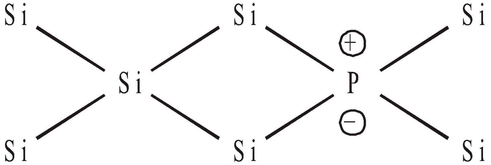
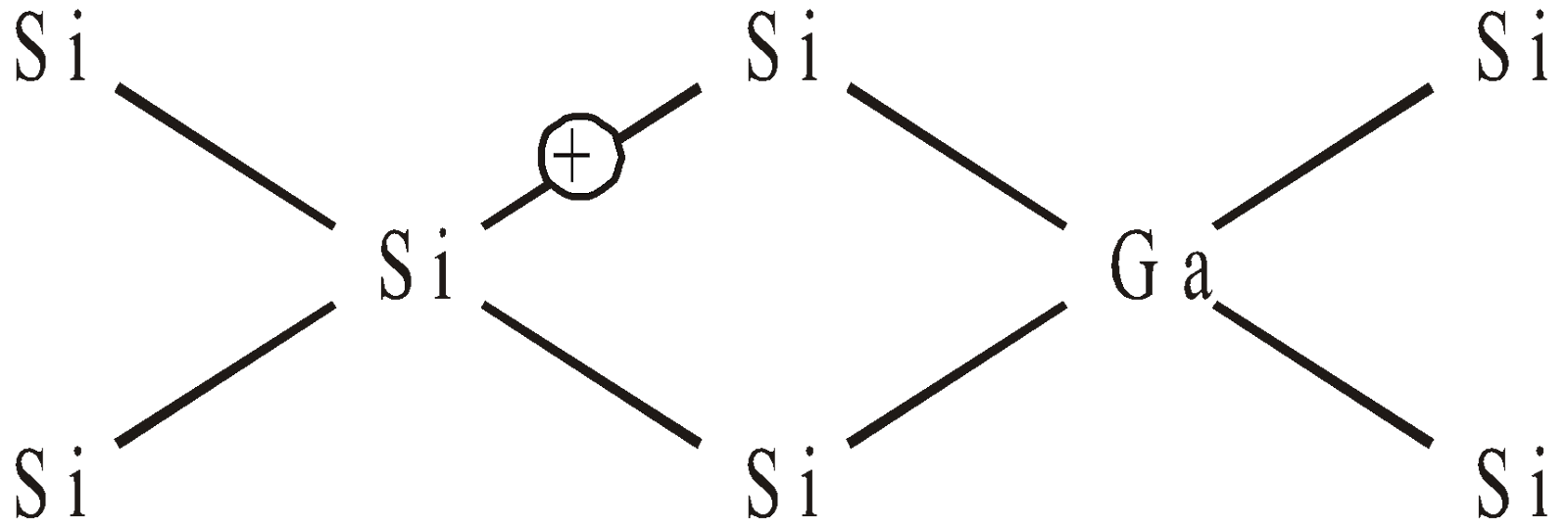
Their conductivity is due to the presence of impurities. They are formed by doping e.g. Si doped with P.
DOPING
It is defined as addition of impurities to a semiconductor to increase the conductivity. Doping of Si or Ge is carried out with P, As, Sb, B, Al or Ga.
DONORS
Impurities capable of donating electrons are known as donors e.g. P, As, Sb.
ACCEPTORS
Impurities capable of accepting electrons are known as acceptors e.g. B, Al, Ga.
N-TYPE SEMICONDUCTORS
Silicon doped with phosphorus is called n-type semiconductor.
The conductivity is due to presence of negative charge (electrons).
P-TYPE SEMICONDUCTORS
Silicon doped with gallium is called p-type semiconductor.
The conductivity is due to the presence of positive holes.
Some typical 13-15 compounds are InSb, AlP and GaAs and some typical 12-16 compounds are ZnS, CdS, CdSe and HgTe.
These exhibit electrical and optical properties of great use in electronic industry.
PIEZOELECTRIC EFFECT AND PIEZOELECTRICITY
The charge developed on the crystal due to mechanical stress is called piezoelectric effect and the current thus produced is called piezo electricity.
PYROELECTRICITY
The electric current produced by heating on the faces of a crystal is called pyroelectricity.
FERROELECTRIC EFFECT
The reversal of direction of permanently lined up dipoles of piezoelectric crystal by applying electric field is called ferro electric effect.
Examples Rochelle Salt, KH2PO4 and Barium titanate BaTiO3.
ANTIFERROELECTRIC SOLID
When the dipoles in alternate lattices point are in opposite direction and net dipole moment is zero, the crystals are referred to as antiferroelectric. Example is lead Zirconate PbZrO3.
DIAMAGNETIC
The substances which are weakly repelled by magnetic fields e.g. KCl, NaCl and TiO2. It is independent of temperature.
PARAMAGNETIC
The substances which are attracted by magnetic field and loss magnetism in the absence of a magnetic field e.g. O2, Cu++, Fe+++, Na, K etc.
FERROMAGNETIC
The substances which are strongly attracted by magnetic field and retain magnetism even when the magnetic field is removed e.g. CrO2, Fe, Co & Ni show ferromagnetism at room temperature. The alignment of magnetic moments is spontaneous in such substances ⬆️ ⬆️ ⬆️ ⬆️ ⬆️ ⬆️
ANTIFERRO MAGNETISM
It is due to compensatory alignment of moments ⬆️ ⬇️ ⬆️ ⬇️ ⬆️ ⬇️ The net moment is zero e.g. MnO, MnSe and KMnFe3.
FERRIMAGNETISM
The alignment of moments are parallel and anti-parallel unequal in number, there is net moment e.g. Fe3O4, ferrites of formula M2+ Fe2O4 (M = Mg, Cu, Zn)
CLASSIFICATION OF SOLIDS ON THE BASIS OF ELECTRICAL CONDUCTIVITY
- Metals : 108 ohm–1 cm–1
- Insulators : 10–12 ohm–1 cm–1
- Semiconductors : 104 – 10–7 ohm–1 cm–1
BERTHOLLIDES
Non Stoichiometric compounds are called Berthollides. The common are sulphides and oxides e.g. FeO, CuO.
LIQUID CRYSTALS (MESOMORPHIC OR PARA CRYSTALLINE)
The substances having the properties of crystalline solids and flow properties of liquids. Examples : Para-azoxyanisole and Normal Octyl-para azoxy cinnamate. Such solids undergo two sharp phase transformations on fusion, first yielding turbid liquid and at higher temperature a clear liquid. The turbid liquids are called liquid crystals and are anisotropic in nature (a property of crystalline solid).
TRANSITION POINT
It is the temperature at which a substance changes sharply into the state of liquid crystals.
POLYMORPHISM
Existence of a substance in more than one crystalline form is known as polymorphism e.g. Carbon, Sulphur, Tin etc.
ALLOTROPY
The polymorphism in elements is known as allotropy.
ENANTIOTROPIC SUBSTANCE
Polymorphic form of a substance whose transition temperature is lower than the fusion temperature is known enantiotropic substance and phenomenon is called enantiotropy.
MONOTROPY
When fusion temperature of both the forms is below the transition temperature the phenomenon is known as monotropy.
ISOMORPHISM
Two or more substances having the same crystalline form are known as isomorphous and the phenomenon is called isomorphism K2SO4.Cr2(SO4)3.24H2O and K2SO4.Al2(SO4)3.24H2O are isomorphous.
MITSCHERLICH'S LAW
It states that isomorphous substances possess an equal number of atoms united in a similar way.
ISOPOLYMORPHISM
When each form of a polymorphic substance is isomorphous with a form of another polymorphic substance the phenomenon is known as Isopolymorphism e.g. antimony trioxide and arsenious oxide both exist in rhombic and octahedral form. The rhombic forms of two oxides are isomorphous and octahedral forms of the oxides are also isomorphous.
SILICATES
Silicates are metal derivatives of silicic acid H4SiO4 obtained by fusing metal oxides or metal carbonates with sand.
CLASSIFICATION OF SILICATES
ORTHO SILICATES
They contain discrete SiO44– units. Metal cations are tetrahedrally surrounded by four O atoms.
Examples : Phenacite Be2SiO4, willemite Zn2SiO4.
PYRO SILICATES
Two tetrahedral units are joined by one oxygen atom and contain Si2O76– unit.
Example : Thortveitite Se2 (Si2O7), Hemimorphite Zn3 (Si2O7) . Zn (OH)2. H2O.
CHAIN SILICATES
(SiO32–)n Two oxygen atoms per SiO4 tetrahedron are shared giving polymeric anion chains.
Example : Spodumene LiAl (SiO3)2, Diposide CaMg(SiO3)2.
(Si4O116–)n contain double chain.
Example : Tremolite Ca2Mg5 (Si4O11) (OH)2.
CYCLIC SILICATES
Two oxygens per SiO4 tetrahedron are shared containing Si3O96– and Si6O1812– units.
Example : Benyl Be3Al2Si6O18
SHEET SILICATES
Here three oxygens of each SiO4 tetrahedron are shared. Containing (Si2O52–)n
Example : Clay.
FRAMEWORK SILICATES
All oxygen atoms of each SiO4 tetrahedron are shared. They contain three dimensional network.
Example : Quartz, zeolite.
Study Notes for JEE Main/JEE Advanced


Study Notes for NEET/AIIMS


